High-electron-mobility transistor


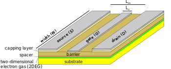
A High-electron-mobility transistor (HEMT), also known as heterostructure FET (HFET) or modulation-doped FET (MODFET), is a field-effect transistor incorporating a junction between two materials with different band gaps (i.e. a heterojunction) as the channel instead of a doped region (as is generally the case for MOSFET). A commonly used material combination is GaAs with AlGaAs, though there is wide variation, dependent on the application of the device. Devices incorporating more indium generally show better high-frequency performance, while in recent years, gallium nitride HEMTs have attracted attention due to their high-power performance. Like other FETs, HEMTs are used in integrated circuits as digital on-off switches. FETs can also be used as amplifiers for large amounts of current using a small voltage as a control signal. Both of these uses are made possible by the FET’s unique current-voltage characteristics. HEMT transistors are able to operate at higher frequencies than ordinary transistors, up to millimeter wave frequencies, and are used in high-frequency products such as cell phones, satellite television receivers, voltage converters, and radar equipment. They are widely used in satellite receivers, in low power amplifiers and in the defense industry.
Advantages
Advantages of HEMTs are that they have:
- high gain. This makes them useful as amplifiers.
- high switching speeds, which are achieved because the main charge carriers in MODFETs are majority carriers, and minority carriers are not significantly involved.
- extremely low noise values because the current variation in these devices is low compared to other FETs.
Invention
The invention of the HEMT is usually attributed to Takashi Mimura (三村 高志) (Fujitsu, Japan).[1] In America, Ray Dingle and his co-workers in Bell Laboratories also played an important role in the invention of the HEMT. Daniel Delagebeaudeuf and Trong Linh Nuyen from Thomson-CSF (France) filed for a patent of this device in March 1979[2]
Conceptual analysis
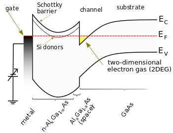
HEMTs are heterojunctions. This means that the semiconductors used have dissimilar band gaps. For instance, silicon has a band gap of 1.1 electron volts (eV), while germanium has a band gap of .67 eV. When a heterojunction is formed, the conduction band and valence band throughout the material must bend in order to form a continuous level.
HEMTs' exceptional carrier mobility and switching speed come from the following conditions. The wide band element is doped with donor atoms; thus it has excess electrons in its conduction band. These electrons will diffuse to the adjacent narrow band material’s conduction band due to the availability of states with lower energy. The movement of electrons will cause a change in potential and thus an electric field between the materials. The electric field will push electrons back to the wide band element’s conduction band. The diffusion process continues until electron diffusion and electron drift balance each other, creating a junction at equilibrium similar to a p-n junction. Note that the undoped narrow band gap material now has excess majority charge carriers. The fact that the charge carriers are majority carriers yields high switching speeds, and the fact that the low band gap semiconductor is undoped means that there are no donor atoms to cause scattering and thus yields high mobility.
An important aspect of HEMTs is that the band discontinuities across the conduction and valence bands can be modified separately. This allows the type of carriers in and out of the device to be controlled. As HEMTs require electrons to be the main carriers, a graded doping can be applied in one of the materials making the conduction band discontinuity smaller, and keeping the valence band discontinuity the same. This diffusion of carriers leads to the accumulation of electrons along the boundary of the two regions inside the narrow band gap material. The accumulation of electrons leads to a very high current in these devices. The accumulated electrons are also known as 2DEG or two-dimensional electron gas.
The term "modulation doping" refers to the fact that the dopants are spatially in a different region from the current carrying electrons. This technique was invented by Horst Störmer at Bell Labs.
Explanation
To allow conduction, semiconductors are doped with impurities which donate either mobile electrons or holes. However, these electrons are slowed down through collisions with the impurities (dopants) used to generate them in the first place. HEMTs avoid this through the use of high mobility electrons generated using the heterojunction of a highly doped wide-bandgap n-type donor-supply layer (AlGaAs in our example) and a non-doped narrow-bandgap channel layer with no dopant impurities (GaAs in this case).
The electrons generated in the thin n-type AlGaAs layer drop completely into the GaAs layer to form a depleted AlGaAs layer, because the heterojunction created by different band-gap materials forms a quantum well (a steep canyon) in the conduction band on the GaAs side where the electrons can move quickly without colliding with any impurities because the GaAs layer is undoped, and from which they cannot escape. The effect of this is to create a very thin layer of highly mobile conducting electrons with very high concentration, giving the channel very low resistivity (or to put it another way, "high electron mobility").
Electrostatic mechanism
Since GaAs has higher electron affinity, free electrons in the AlGaAs layer are transferred to the undoped GaAs layer where they form a two dimensional high mobility electron gas within 100 ångström (10 nm) of the interface. The n-type AlGaAs layer of the HEMT is depleted completely through two depletion mechanisms:
- Trapping of free electrons by surface states causes the surface depletion.
- Transfer of electrons into the undoped GaAs layer brings about the interface depletion.
The Fermi level of the gate metal is matched to the pinning point, which is 1.2 eV below the conduction band. With the reduced AlGaAs layer thickness, the electrons supplied by donors in the AlGaAs layer are insufficient to pin the layer. As a result, band bending is moving upward and the two-dimensional electrons gas does not appear. When a positive voltage greater than the threshold voltage is applied to the gate, electrons accumulate at the interface and form a two-dimensional electron gas.
Manufacture
MODFETs can be manufactured by epitaxial growth of a strained SiGe layer. In the strained layer, the germanium content increases linearly to around 40-50%. This concentration of germanium allows the formation of a quantum well structure with a high conduction band offset and a high density of very mobile charge carriers. The end result is a FET with ultra-high switching speeds and low noise. InGaAs/AlGaAs, AlGaN/InGaN, and other compounds are also used in place of SiGe. InP and GaN are starting to replace SiGe as the base material in MODFETs because of their better noise and power ratios.
Versions of HEMTs
pHEMT
Ideally, the two different materials used for a heterojunction would have the same lattice constant (spacing between the atoms). In practice, the lattice constants are typically slightly different (e.g. AlGaAs on GaAs), resulting in crystal defects. As an analogy, imagine pushing together two plastic combs with a slightly different spacing. At regular intervals, you'll see two teeth clump together. In semiconductors, these discontinuities form deep-level traps and greatly reduce device performance.
A HEMT where this rule is violated is called a pHEMT or pseudomorphic HEMT. This is achieved by using an extremely thin layer of one of the materials – so thin that the crystal lattice simply stretches to fit the other material. This technique allows the construction of transistors with larger bandgap differences than otherwise possible, giving them better performance.[3]
mHEMT
Another way to use materials of different lattice constants is to place a buffer layer between them. This is done in the mHEMT or metamorphic HEMT, an advancement of the pHEMT. The buffer layer is made of AlInAs, with the indium concentration graded so that it can match the lattice constant of both the GaAs substrate and the GaInAs channel. This brings the advantage that practically any Indium concentration in the channel can be realized, so the devices can be optimized for different applications (low indium concentration provides low noise; high indium concentration gives high gain).
Induced HEMT
In contrast to a modulation-doped HEMT, an induced high electron mobility transistor provides the flexibility to tune different electron densities with a top gate, since the charge carriers are "induced" to the 2DEG plane rather than created by dopants. The absence of a doped layer enhances the electron mobility significantly when compared to their modulation-doped counterparts. This level of cleanliness provides opportunities to perform research into the field of Quantum Billiard for quantum chaos studies, or applications in ultra stable and ultra sensitive electronic devices.
Applications
Applications (eg for AlGaAs on GaAs) are similar to those of MESFETs – microwave and millimeter wave communications, imaging, radar, and radio astronomy – any application where high gain and low noise at high frequencies are required. HEMTs have shown current gain to frequencies greater than 600 GHz and power gain to frequencies greater than 1 THz.[4] (Heterojunction bipolar transistors were demonstrated at current gain frequencies over 600 GHz in April 2005.) Numerous companies worldwide develop and manufacture HEMT-based devices. These can be discrete transistors but are more usually in the form of a 'monolithic microwave integrated circuit' (MMIC). HEMTs are found in many types of equipment ranging from cellphones and DBS receivers to electronic warfare systems such as radar and for radio astronomy.
Furthermore, gallium nitride HEMTs on silicon substrates are used as power switching transistors for voltage converter applications. Compared to silicon power transistors gallium nitride HEMTs feature low on-state resistances, and low switching losses due to the wide bandgap properties. Gallium nitride power HEMTs are commercially available up to voltages of 200 V-600 V.
See also
References
- ↑ Takashi Mimura: 'The Early History of the High Electron Mobility Transistor (HEMT)',IEEE TRANSACTIONS ON MICROWAVE THEORY AND TECHNIQUES, VOL. 50, NO. 3, MARCH 2002,.
- ↑ US 4471366, Daniel Delagebeaudeuf and Trong L. Nuyen, "Field effect transistor with high cut-off frequency and process for forming same" google patents link
- ↑ Indium Phosphide: Transcending frequency and integration limits. Semiconductor TODAY Compounds&AdvancedSilicon • Vol. 1 • Issue 3 • September 2006
- ↑ http://www.semiconductor-today.com/news_items/2014/OCT/NORTHROP-GRUMMAN_311014.shtml