Crystallographic defect

Crystalline solids exhibit a periodic crystal structure. The positions of atoms or molecules occur on repeating fixed distances, determined by the unit cell parameters. However, the arrangement of atoms or molecules in most crystalline materials is not perfect. The regular patterns are interrupted by crystallographic defects.[2][3][4][5]
Point defects
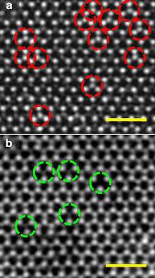
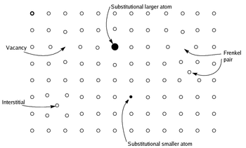
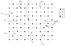
Point defects are defects that occur only at or around a single lattice point. They are not extended in space in any dimension. Strict limits for how small a point defect is are generally not defined explicitly, typically, however, these defects involve at most a few extra or missing atoms. Larger defects in an ordered structure are usually considered dislocation loops. For historical reasons, many point defects, especially in ionic crystals, are called centers: for example a vacancy in many ionic solids is called a luminescence center, a color center, or F-center. These dislocations permit ionic transport through crystals leading to electrochemical reactions. These are frequently specified using Kröger–Vink Notation.
- Vacancy defects are lattice sites which would be occupied in a perfect crystal, but are vacant. If a neighboring atom moves to occupy the vacant site, the vacancy moves in the opposite direction to the site which used to be occupied by the moving atom. The stability of the surrounding crystal structure guarantees that the neighboring atoms will not simply collapse around the vacancy. In some materials, neighboring atoms actually move away from a vacancy, because they experience attraction from atoms in the surroundings. A vacancy (or pair of vacancies in an ionic solid) is sometimes called a Schottky defect.
- Interstitial defects are atoms that occupy a site in the crystal structure at which there is usually not an atom. They are generally high energy configurations. Small atoms in some crystals can occupy interstices without high energy, such as hydrogen in palladium.

- A nearby pair of a vacancy and an interstitial is often called a Frenkel defect or Frenkel pair. This is caused when an ion moves into an interstitial site and creates a vacancy.
- Due to fundamental limitations of material purification methods, materials are never 100% pure, which by definition induces defects in crystal structure. In the case of an impurity, the atom is often incorporated at a regular atomic site in the crystal structure. This is neither a vacant site nor is the atom on an interstitial site and it is called a substitutional defect. The atom is not supposed to be anywhere in the crystal, and is thus an impurity. In some cases where the radius of the substitutional atom (ion) is substantially smaller than that of the atom (ion) it is replacing, its equilibrium position can be shifted away from the lattice site. These types of substitutional defects are often referred to as off-center ions. There are two different types of substitutional defects: Isovalent substitution and aliovalent substitution. Isovalent substitution is where the ion that is substituting the original ion is of the same oxidation state as the ion it is replacing. Aliovalent substitution is where the ion that is substituting the original ion is of a different oxidation state than the ion it is replacing. Aliovalent substitutions change the overall charge within the ionic compound, but the ionic compound must be neutral. Therefore, a charge compensation mechanism is required. Hence either one of the metals is partially or fully oxidised or reduced, or ion vacancies are created.
- Antisite defects[6][7] occur in an ordered alloy or compound when atoms of different type exchange positions. For example, some alloys have a regular structure in which every other atom is a different species; for illustration assume that type A atoms sit on the corners of a cubic lattice, and type B atoms sit in the center of the cubes. If one cube has an A atom at its center, the atom is on a site usually occupied by a B atom, and is thus an antisite defect. This is neither a vacancy nor an interstitial, nor an impurity.
- Topological defects are regions in a crystal where the normal chemical bonding environment is topologically different from the surroundings. For instance, in a perfect sheet of graphite (graphene) all atoms are in rings containing six atoms. If the sheet contains regions where the number of atoms in a ring is different from six, while the total number of atoms remains the same, a topological defect has formed. An example is the Stone Wales defect in nanotubes, which consists of two adjacent 5-membered and two 7-membered atom rings.

- Also amorphous solids may contain defects. These are naturally somewhat hard to define, but sometimes their nature can be quite easily understood. For instance, in ideally bonded amorphous silica all Si atoms have 4 bonds to O atoms and all O atoms have 2 bonds to Si atom. Thus e.g. an O atom with only one Si bond (a dangling bond) can be considered a defect in silica.[8] Moreover, defects can also be defined in amorphous solids based on empty or densely packed local atomic neighbourhoods, and the properties of such 'defects' can be shown to be similar to normal vacancies and interstitials in crystals,.[9][10][11]
- Complexes can form between different kinds of point defects. For example, if a vacancy encounters an impurity, the two may bind together if the impurity is too large for the lattice. Interstitials can form 'split interstitial' or 'dumbbell' structures where two atoms effectively share an atomic site, resulting in neither atom actually occupying the site.
Line defects
Line defects can be described by gauge theories.
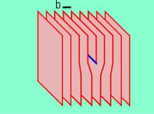
Dislocations are linear defects around which some of the atoms of the crystal lattice are misaligned.[12] There are two basic types of dislocations, the edge dislocation and the screw dislocation. "Mixed" dislocations, combining aspects of both types, are also common.

Edge dislocations are caused by the termination of a plane of atoms in the middle of a crystal. In such a case, the adjacent planes are not straight, but instead bend around the edge of the terminating plane so that the crystal structure is perfectly ordered on either side. The analogy with a stack of paper is apt: if a half a piece of paper is inserted in a stack of paper, the defect in the stack is only noticeable at the edge of the half sheet.
The screw dislocation is more difficult to visualise, but basically comprises a structure in which a helical path is traced around the linear defect (dislocation line) by the atomic planes of atoms in the crystal lattice.
The presence of dislocation results in lattice strain (distortion). The direction and magnitude of such distortion is expressed in terms of a Burgers vector (b). For an edge type, b is perpendicular to the dislocation line, whereas in the cases of the screw type it is parallel. In metallic materials, b is aligned with close-packed crystallographic directions and its magnitude is equivalent to one interatomic spacing.
Dislocations can move if the atoms from one of the surrounding planes break their bonds and rebond with the atoms at the terminating edge.
It is the presence of dislocations and their ability to readily move (and interact) under the influence of stresses induced by external loads that leads to the characteristic malleability of metallic materials.
Dislocations can be observed using transmission electron microscopy, field ion microscopy and atom probe techniques. Deep level transient spectroscopy has been used for studying the electrical activity of dislocations in semiconductors, mainly silicon.
Disclinations are line defects corresponding to "adding" or "subtracting" an angle around a line. Basically, this means that if you track the crystal orientation around the line defect, you get a rotation. Usually, they were thought to play a role only in liquid crystals, but recent developments suggest that they might have a role also in solid materials, e.g. leading to the self-healing of cracks.[13]
Planar defects

- Grain boundaries occur where the crystallographic direction of the lattice abruptly changes. This usually occurs when two crystals begin growing separately and then meet.
- Antiphase boundaries occur in ordered alloys: in this case, the crystallographic direction remains the same, but each side of the boundary has an opposite phase: For example, if the ordering is usually ABABABAB (hexagonal close-packed crystal), an antiphase boundary takes the form of ABABBABA.
- Stacking faults occur in a number of crystal structures, but the common example is in close-packed structures. They are formed by a local deviation of the stacking sequence of layers in a crystal. An example would be the ABABCABAB stacking sequence.
- A twin boundary is a defect that introduces a plane of mirror symmetry in the ordering of a crystal. For example, in cubic close-packed crystals, the stacking sequence of a twin boundary would be ABCABCBACBA.
- On surfaces of single crystals, steps between atomically flat terraces can also be regarded as planar defects. It has been shown that such defects and their geometry have significant influence on the adsorption of organic molecules[14]
Bulk defects
- three-dimensional macroscopic or bulk defects, such as pores, cracks, or inclusions
- Voids — small regions where there are no atoms, and which can be thought of as clusters of vacancies
- Impurities can cluster together to form small regions of a different phase. These are often called precipitates.
Mathematical classification methods
A successful mathematical classification method for physical lattice defects, which works not only with the theory of dislocations and other defects in crystals but also, e.g., for disclinations in liquid crystals and for excitations in superfluid 3He, is the topological homotopy theory.[15]
Computer simulation methods
Density functional theory, classical molecular dynamics and kinetic Monte Carlo [16] simulations are widely used to study the properties of defects in solids with computer simulations.[9][10][11][17][18][19][20] Simulating jamming of hard spheres of different sizes and/or in containers with non-commeasurable sizes using the Lubachevsky–Stillinger algorithm can be an effective technique for demonstrating some types of crystallographic defects.[21]
See also
References
- ↑ Hong, J.; Hu, Z.; Probert, M.; Li, K.; Lv, D.; Yang, X.; Gu, L.; Mao, N.; Feng, Q.; Xie, L.; Zhang, J.; Wu, D.; Zhang, Z.; Jin, C.; Ji, W.; Zhang, X.; Yuan, J.; Zhang, Z. (2015). "Exploring atomic defects in molybdenum disulphide monolayers". Nature Communications. 6: 6293. Bibcode:2015NatCo...6E6293H. doi:10.1038/ncomms7293. PMC 4346634
 . PMID 25695374.
 - ↑ Ehrhart, P. (1991) Properties and interactions of atomic defects in metals and alloys, volume 25 of Landolt-Börnstein, New Series III, chapter 2, p. 88, Springer, Berlin
- ↑ Siegel, R. W. (1982) Atomic Defects and Diffusion in Metals, in Point Defects and Defect Interactions in Metals, J.-I. Takamura (ED.), p. 783, North Holland, Amsterdam
- ↑ Crawford, J. H.; Slifkin, L. M., eds. (1975). Point Defects in Solids. New York: Plenum Press.
- ↑ Watkins, G. D. (1997) "Native defects and their interactions with impurities in silicon", p. 139 in Defects and Diffusion in Silicon Processing, T. Diaz de la Rubia, S. Coffa, P. A. Stolk, and C. S. Rafferty (eds), vol. 469 of MRS Symposium Proceedings, Materials Research Society, Pittsburgh, ISBN 1-55899-373-8
- ↑ Mattila, T; Nieminen, RM (1995). "Direct Antisite Formation in Electron Irradiation of GaAs". Physical Review Letters. 74 (14): 2721–2724. Bibcode:1995PhRvL..74.2721M. doi:10.1103/PhysRevLett.74.2721. PMID 10058001.
- ↑ Hausmann, H.; Pillukat, A.; Ehrhart, P. (1996). "Point defects and their reactions in electron-irradiated GaAs investigated by optical absorption spectroscopy". Physical Review B. 54 (12): 8527–8539. Bibcode:1996PhRvB..54.8527H. doi:10.1103/PhysRevB.54.8527.
- ↑ Lieb, Klaus-Peter; Keinonen, Juhani (2006). "Luminescence of ion-irradiated α-quartz". Contemporary Physics. 47 (5): 305–331. Bibcode:2006ConPh..47..305L. doi:10.1080/00107510601088156.
- 1 2 Ashkenazy, Yinon; Averback, Robert S. (2012). "Irradiation Induced Grain Boundary Flow—A New Creep Mechanism at the Nanoscale". Nano Letters. 12 (8): 4084–9. Bibcode:2012NanoL..12.4084A. doi:10.1021/nl301554k. PMID 22775230.
- 1 2 Mayr, S.; Ashkenazy, Y.; Albe, K.; Averback, R. (2003). "Mechanisms of radiation-induced viscous flow: Role of point defects". Phys. Rev. Lett. 90 (5): 055505. Bibcode:2003PhRvL..90e5505M. doi:10.1103/PhysRevLett.90.055505. PMID 12633371.
- 1 2 Nordlund, K; Ashkenazy, Y; Averback, R. S; Granato, A. V (2005). "Strings and interstitials in liquids, glasses and crystals". Europhys. Lett. 71 (4): 625–631. Bibcode:2005EL.....71..625N. doi:10.1209/epl/i2005-10132-1.
- ↑ Hirth, J. P.; Lothe, J. (1992). Theory of dislocations (2 ed.). Krieger Pub Co. ISBN 0-89464-617-6.
- ↑ Chandler, David L., Cracked metal, heal thyself, MIT news, October 9, 2013
- ↑ Waldmann, T. (2012). "The role of surface defects in large organic molecule adsorption: substrate configuration effects". Physical Chemistry Chemical Physics. 14 (30): 10726–31. Bibcode:2012PCCP...1410726W. doi:10.1039/C2CP40800G. PMID 22751288.
- ↑ Mermin, N. (1979). "The topological theory of defects in ordered media". Reviews of Modern Physics. 51 (3): 591–648. Bibcode:1979RvMP...51..591M. doi:10.1103/RevModPhys.51.591.
- ↑ Cai, W.; Bulatov, V. V.; Justo, J. F.; Argon, A.S,; Yip, S. (2000). "Intrinsic mobility of a dissociated dislocation in silicon". Phys. Rev. Lett. 84 (15): 3346–3349. Bibcode:2000PhRvL..84.3346C. doi:10.1103/PhysRevLett.84.3346. PMID 11019086.
- ↑ Korhonen, T; Puska, M.; Nieminen, R. (1995). "Vacancy formation energies for fcc and bcc transition metals". Phys. Rev. B. 51 (15): 9526–9532. Bibcode:1995PhRvB..51.9526K. doi:10.1103/PhysRevB.51.9526.
- ↑ Puska, M. J.; Pöykkö, S.; Pesola, M.; Nieminen, R. (1998). "Convergence of supercell calculations for point defects in semiconductors: vacancy in silicon". Phys. Rev. B. 58 (3): 1318–1325. Bibcode:1998PhRvB..58.1318P. doi:10.1103/PhysRevB.58.1318.
- ↑ Nordlund, K.; Averback, R. (1998). "The role of self-interstitial atoms on the high temperature properties of metals". Phys. Rev. Lett. 80 (19): 4201–4204. Bibcode:1998PhRvL..80.4201N. doi:10.1103/PhysRevLett.80.4201.
- ↑ Sadigh, B; Lenosky, Thomas; Theiss, Silva; Caturla, Maria-Jose; Diaz De La Rubia, Tomas; Foad, Majeed (1999). "Mechanism of Boron Diffusion in Silicon: An Ab Initio and Kinetic Monte Carlo Study". Phys. Rev. Lett. 83 (21): 4341–4344. Bibcode:1999PhRvL..83.4341S. doi:10.1103/PhysRevLett.83.4341.
- ↑ Stillinger, Frank H.; Lubachevsky, Boris D. (1995). "Patterns of broken symmetry in the impurity-perturbed rigid-disk crystal". Journal of Statistical Physics. 78 (3–4): 1011–1026. Bibcode:1995JSP....78.1011S. doi:10.1007/BF02183698.
Further reading
- Hagen Kleinert, Gauge Fields in Condensed Matter, Vol. II, "Stresses and defects", pp. 743–1456, World Scientific (Singapore, 1989); Paperback ISBN 9971-5-0210-0
- Hermann Schmalzried: Solid State Reactions. Verlag Chemie, Weinheim 1981, ISBN 3-527-25872-8.